
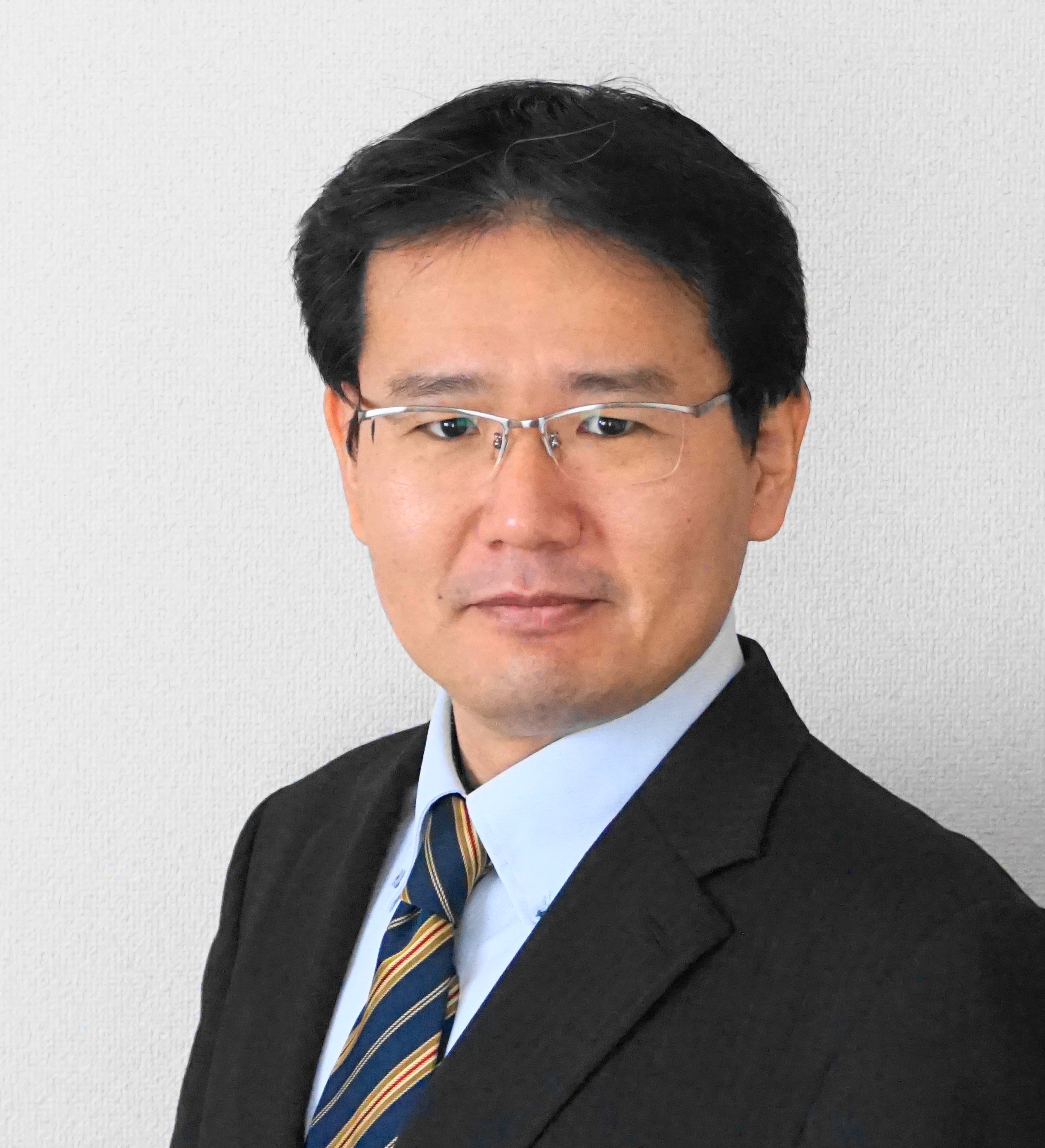
Munehiro TADA
タダ ムネヒロ
Munehiro TADA
Faculty of Science and Technology Department of System Design Engineering/ProfessorBasic Information
Specialty
Heterogeneous integrated systems, Semiconductor devices, Multi-level interconnects, Neuromorphic circuits, Cryo-CMOS for controlling qubits
Related Links
Researcher Number
20607890
Laboratory Information
Paper Review Qualification
Thesis Guide Qualification in the Graduate School of Science and Technology : Master/Doctor
Message from Faculty
After completing my graduate studies, I joined a private company and have been involved in semiconductor research and product development for over 20 years. During this time, I experienced numerous transfers, including studying abroad in the United States and being seconded to research associations, where I worked alongside people with diverse perspectives and approaches. In 2019, I founded a startup, and since 2024, I have been engaged at this institution. I aim to leverage my professional experience in the private sector to contribute to education.
Biography
Researcher profile
Munehiro Tada received the M.S. and Ph.D. degrees from Keio University, Japan, in 1999 and 2007, respectively. He joined NEC Corporation, Japan, in 1999. From 2007 to 2008, he was a visiting scholar at Stanford University. From 2019, he is a cofounder and executive board director at NanoBridge Semiconductor, Inc. From 2024, he is a full professor at Keio University. He published papers with 16-IEDM, 17-VLSI and 11-IITC. He hold more than 100 issued patents. He is an IEEE Fellow and a JSAP Fellow. He is an adviser at JST-CREST(2020-), an executive board director at JSAP(2024-2025), a board director at NanoBridge Semiconductor, Inc.(2019-), a director at Yagami Innovation Laboratory in Keio University (2025-), and IEEE Fellow Commitee Member(2026-).
General introduction
To address the limitations of semiconductor miniaturization technology, I aim to achieve low-power, high-performance information processing and integrated systems by combining new nanodevices with heterogeneous technologies. With a focus on optimizing systems, I am working on areas such as advanced fine wiring technologies, brain-inspired "brains-in-silicon" circuits using atomic switches, efficient cooling technologies for three-dimensional stacked chips, and quantum bit control systems at cryogenic temperatures.
Research
Reseach overview
For approaching limits to semiconductor miniaturization technology, we are aiming to construct a low-power and high-performance integrated information processing system by combining heterogeneous technologies and incorporating novel nanodevices. Specifically, we are focusing on an embedded memory, a development of neuromorphic circuits that mimic a functionality of brain's neural networks and systems that control quantum bit at cryogenic temperatures.
Research Interests
- Semiconductor device engineering
- ヘテロジーニアス集積システム
- 原子スイッチ・ナノブリッジ
Research areas
Electron device and electronic equipment / Semiconductor Device Engineering